
David cherns (16 risultati)

- Rilegato
- Prima edizione
Da: Reader's Corner, Inc., Raleigh, NC, U.S.A.Reader's Corner, Inc.
Contatta il venditoreVenditore con 5 stelleCondizione: Usato - Come nuovo
EUR 9,16
EUR 4,89 spedizioneSpedito in U.S.A.Quantità: 1 disponibile
Hardcover. Condizione: As New. No Jacket. First Edition. Proceedings of the institute of physics electron microscopy and analysis group conference, university of birmingham 12-15 september 1995. Slick gray hardcover binding, no DJ. Like new copy.

- Brossura
Da: Kennys Bookstore, Olney, MD, U.S.A.Kennys Bookstore
Contatta il venditoreVenditore con 5 stelleCondizione: Usato - Molto buono
EUR 19,36
EUR 9,34 spedizioneSpedito in U.S.A.Quantità: 1 disponibile
Condizione: Very Good. 1976. Paperback. Ex Libris with usual markings. Clean copy with some minor shelf wear, minor edge wear and sunning to spine. . . . . Books ship from the US and Ireland.
- Brossura
Da: Kennys Bookshop and Art Galleries Ltd., Galway, GY, IrlandaKennys Bookshop and Art Galleries Ltd.
Contatta il venditoreVenditore con 5 stelleCondizione: Usato - Molto buono
EUR 21,54
EUR 9,50 spedizioneSpedito da Irlanda a U.S.A.Quantità: 1 disponibile
Condizione: Very Good. 1976. Paperback. Ex Libris with usual markings. Clean copy with some minor shelf wear, minor edge wear and sunning to spine. . . . .
- Brossura
Da: GreatBookPrices, Columbia, MD, U.S.A.GreatBookPrices
Contatta il venditoreVenditore con 5 stelleCondizione: Nuovo
EUR 53,63
EUR 2,35 spedizioneSpedito in U.S.A.Quantità: 15 disponibili
Condizione: New.

- Brossura
Da: Ria Christie Collections, Uxbridge, Regno UnitoRia Christie Collections
Contatta il venditoreVenditore con 5 stelleCondizione: Nuovo
EUR 68,35
EUR 13,39 spedizioneSpedito da Regno Unito a U.S.A.Quantità: Più di 20 disponibili
Condizione: New. In English.

- Brossura
Da: GreatBookPrices, Columbia, MD, U.S.A.GreatBookPrices
Contatta il venditoreVenditore con 5 stelleCondizione: Usato - Come nuovo
EUR 144,48
EUR 2,35 spedizioneSpedito in U.S.A.Quantità: 15 disponibili
Condizione: As New. Unread book in perfect condition.
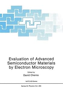
Evaluation of Advanced Semiconductor Materials by Electron Microscopy (Nato Science Series B: (203))
- Brossura
Da: Mispah books, Redhill, SURRE, Regno UnitoMispah books
Contatta il venditoreVenditore con 4 stelleCondizione: Usato - Come nuovo
EUR 123,38
EUR 29,65 spedizioneSpedito da Regno Unito a U.S.A.Quantità: 1 disponibile
Paperback. Condizione: Like New. LIKE NEW. SHIPS FROM MULTIPLE LOCATIONS. book.

- Rilegato
Da: Solr Books, Lincolnwood, IL, U.S.A.Solr Books
Contatta il venditoreVenditore con 5 stelleCondizione: Usato - Buono
EUR 305,15
EUR 7,10 spedizioneSpedito in U.S.A.Quantità: 1 disponibile
Condizione: good. This book is in Good condition. There may be some notes and highligting but otherwise the book is in overall good condition.

- Rilegato
Da: Buchpark, Trebbin, GermaniaBuchpark
Contatta il venditoreVenditore con 5 stelleCondizione: Usato - Ottimo
EUR 589,00
EUR 105,00 spedizioneSpedito da Germania a U.S.A.Quantità: 2 disponibili
Condizione: Sehr gut. Zustand: Sehr gut | Seiten: 412 | Sprache: Englisch | Produktart: Bücher | Keine Beschreibung verfügbar.
- Brossura
- Print on Demand
Da: Brook Bookstore On Demand, Napoli, NA, ItaliaBrook Bookstore On Demand
Contatta il venditoreVenditore con 5 stelleCondizione: Nuovo
EUR 46,22
EUR 6,80 spedizioneSpedito da Italia a U.S.A.Quantità: Più di 20 disponibili
Condizione: new. Questo è un articolo print on demand.
- Brossura
- Print on Demand
Da: Chiron Media, Wallingford, Regno UnitoChiron Media
Contatta il venditoreVenditore con 5 stelleCondizione: Nuovo
EUR 58,49
EUR 7,70 spedizioneSpedito da Regno Unito a U.S.A.Quantità: 20 disponibili
PF. Condizione: New. This item is printed on demand. Brand new book, sourced directly from publisher. Dispatch time is 6-7 days from our warehouse. Book will be sent in robust, secure packaging to ensure it reaches you securely.
- Brossura
- Print on Demand
Da: THE SAINT BOOKSTORE, Southport, Regno UnitoTHE SAINT BOOKSTORE
Contatta il venditoreVenditore con 5 stelleCondizione: Nuovo
EUR 70,42
EUR 21,18 spedizioneSpedito da Regno Unito a U.S.A.Quantità: Più di 20 disponibili
Paperback / softback. Condizione: New. This item is printed on demand. New copy - Usually dispatched within 5-9 working days.

- Brossura
- Print on Demand
Da: moluna, Greven, Germaniamoluna
Contatta il venditoreVenditore con 5 stelleCondizione: Nuovo
EUR 48,37
EUR 48,99 spedizioneSpedito da Germania a U.S.A.Quantità: Più di 20 disponibili
Condizione: New. Dieser Artikel ist ein Print on Demand Artikel und wird nach Ihrer Bestellung fuer Sie gedruckt. The last few years have ~een rapid improvements in semiconductor growth techniques which have produced an expanding range of high quality heterostructures for new semiconductor devises. As the dimensions of such structures approach the nanometer level, it b. …

- Brossura
- Print on Demand
Da: AHA-BUCH GmbH, Einbeck, GermaniaAHA-BUCH GmbH
Contatta il venditoreVenditore con 5 stelleCondizione: Nuovo
EUR 66,40
EUR 35,00 spedizioneSpedito da Germania a U.S.A.Quantità: 1 disponibile
Taschenbuch. Condizione: Neu. nach der Bestellung gedruckt Neuware - Printed after ordering - The last few years have ~een rapid improvements in semiconductor growth techniques which have produced an expanding range of high quality heterostructures for new semiconductor devises. As the dimensions of such structures approach the nanometer level, it becomes increasingly important to characterise materials properties such as composition uniformity, strain, interface sharpness and roughness and the nature of defects, as well as their influence on electrical and optical properties. Much of this information is being obtained by electron microscopy and this is also an area of rapid progress. There have been advances for thin film studies across a wide range of techniques, including, for example, convergent beam electron diffraction, X-ray and electron energy loss microanalysis and high spatial resolution cathodoluminescence as well as by conventional and high resolution methods. Important develop ments have also occurred in the study of surfaces and film growth phenomena by both microscopy and diffraction techniques. With these developments in mind, an application was made to the NATO Science Committee in late summer 1987 to fund an Advanced Research Work shop to review the electron microscopy of advanced semiconductors. This was subsequently accepted for the 1988 programme and became the 'NATO Advanced Research Workshop on the Evaluation of Advanced Semiconductor Materials by Electron Microscopy'. The Workshop took place in the pleasant and intimate surroundings of Wills Hall, Bristol, UK, during the week 11-17 September 1988 and was attended by fifty-five participants from fourteen countries.…

- Brossura
- Print on Demand
Da: BuchWeltWeit Ludwig Meier e.K., Bergisch Gladbach, GermaniaBuchWeltWeit Ludwig Meier e.K.
Contatta il venditoreVenditore con 5 stelleCondizione: Nuovo
EUR 85,55
EUR 23,00 spedizioneSpedito da Germania a U.S.A.Quantità: 2 disponibili
Taschenbuch. Condizione: Neu. This item is printed on demand - it takes 3-4 days longer - Neuware -The last few years have ~een rapid improvements in semiconductor growth techniques which have produced an expanding range of high quality heterostructures for new semiconductor devises. As the dimensions of such structures approach the nanometer level, it becomes increasingly important to characterise materials properties such as composition uniformity, strain, interface sharpness and roughness and the nature of defects, as well as their influence on electrical and optical properties. Much of this information is being obtained by electron microscopy and this is also an area of rapid progress. There have been advances for thin film studies across a wide range of techniques, including, for example, convergent beam electron diffraction, X-ray and electron energy loss microanalysis and high spatial resolution cathodoluminescence as well as by conventional and high resolution methods. Important develop ments have also occurred in the study of surfaces and film growth phenomena by both microscopy and diffraction techniques. With these developments in mind, an application was made to the NATO Science Committee in late summer 1987 to fund an Advanced Research Work shop to review the electron microscopy of advanced semiconductors. This was subsequently accepted for the 1988 programme and became the 'NATO Advanced Research Workshop on the Evaluation of Advanced Semiconductor Materials by Electron Microscopy'. The Workshop took place in the pleasant and intimate surroundings of Wills Hall, Bristol, UK, during the week 11-17 September 1988 and was attended by fifty-five participants from fourteen countries. 428 pp. Englisch.…

- Brossura
- Print on Demand
Da: buchversandmimpf2000, Emtmannsberg, BAYE, Germaniabuchversandmimpf2000
Contatta il venditoreVenditore con 5 stelleCondizione: Nuovo
EUR 53,49
EUR 60,00 spedizioneSpedito da Germania a U.S.A.Quantità: 1 disponibile
Taschenbuch. Condizione: Neu. This item is printed on demand - Print on Demand Titel. Neuware -The last few years have ~een rapid improvements in semiconductor growth techniques which have produced an expanding range of high quality heterostructures for new semiconductor devises. As the dimensions of such structures approach the nanometer level, it becomes increasingly important to characterise materials properties such as composition uniformity, strain, interface sharpness and roughness and the nature of defects, as well as their influence on electrical and optical properties. Much of this information is being obtained by electron microscopy and this is also an area of rapid progress. There have been advances for thin film studies across a wide range of techniques, including, for example, convergent beam electron diffraction, X-ray and electron energy loss microanalysis and high spatial resolution cathodoluminescence as well as by conventional and high resolution methods. Important develop ments have also occurred in the study of surfaces and film growth phenomena by both microscopy and diffraction techniques. With these developments in mind, an application was made to the NATO Science Committee in late summer 1987 to fund an Advanced Research Work shop to review the electron microscopy of advanced semiconductors. This was subsequently accepted for the 1988 programme and became the 'NATO Advanced Research Workshop on the Evaluation of Advanced Semiconductor Materials by Electron Microscopy'. The Workshop took place in the pleasant and intimate surroundings of Wills Hall, Bristol, UK, during the week 11-17 September 1988 and was attended by fifty-five participants from fourteen countries.Springer Verlag GmbH, Tiergartenstr. 17, 69121 Heidelberg 428 pp. Englisch.…


